Touting technological expertise as well as a keen eye on market development, ANS takes pride in manufacturing high-quality PCBs for a wide array of applications, including computer-related products, telecommunications items, consumer electronics, power supplies, industrial products, etc.
In terms of technological advancements, we have been able to bring our minimum thickness down to 0.2mm (double-sized), and via hole size down to 0.15mm, while our maximum layer count can reach up to 30. As for the finishes, HASL; HASL (Lead-free); selective Gold, Immersion Gold, Silver and Tin, Palladium Gold; Carbon print; Gold fingers; Entek (OSP); flux coating; peelable mask and LPI are all available.
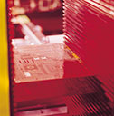
With the increase in popularity of compact personal electronics, there is a tendency for components to become smaller and smaller while being able to perform more sophisticated functions. In light of this, ANS has been emphasizing its production and technological advancements as well as R&D.
We know that one of your main concerns is the confidentiality of your product designs. In this respect, we have strict rules and a secure system to protect the confidentiality of our customers product designs. That is why we have been successful in building up trusting relationships with our clients ever since our inception.